CUBE
During my year in industry at Huawei, it dawned on me how little practical experience I had on engineering projects. I’ve always been into tech and being creative, yet I hadn’t ever taken the dive into trying to build something from scratch. I started by surrounding everything I saw online with other engineers and creators to help inspire ideas. Months went past with me silently browsing and finding new creators, when I found a post by Greg Davill. This colourful cube was exactly the sort of thing I was looking for. It was flashy and “simple enough” to get started. I realized early on that FPGAs were a bit too much for a first time project, so I looked into ways of working with microcontrollers. I also wanted to miniaturize what he had done, so I looked around and found other projects of a similar theme. More reading led me to find Pol Pla’s paper on Display Blocks.
Display Blocks are designed to be a series of handheld devices, enabling easy manipulation. Holding a device in their hands, users are able to easily rotate it and reveal its different sides. Thus, creating a self-enclosed, autonomous device was crucial to offering unencumbered exploration of content. The final design supports not only single device manipulation but also holding multiple devices at once. For this purpose, the devices must be easy to manipulate using only one hand; this way, users can compare cubes side by side, adding even more richness to the navigation of data.
After reading this, I knew this was the project I had to work on, no matter how difficult it might be. Not only would it be a great engineering challenge, but it provided a tangible and satisfying object at the end of it.
Circuit Design
I decided the easiest way to house the electronics for this project was to build 6 PCBs. PCB 1 acts as the motherboard – holding the main circuitry, with PCBs 2-6 acting as daughter boards simply containing the basic passive components and connectors to attach to displays. All of these boards are daisy-chained together using Flat Flex Cables (FFC). These cables act as the bus providing the necessary power and SPI signals to the boards.
Motherboard (PCB 1)
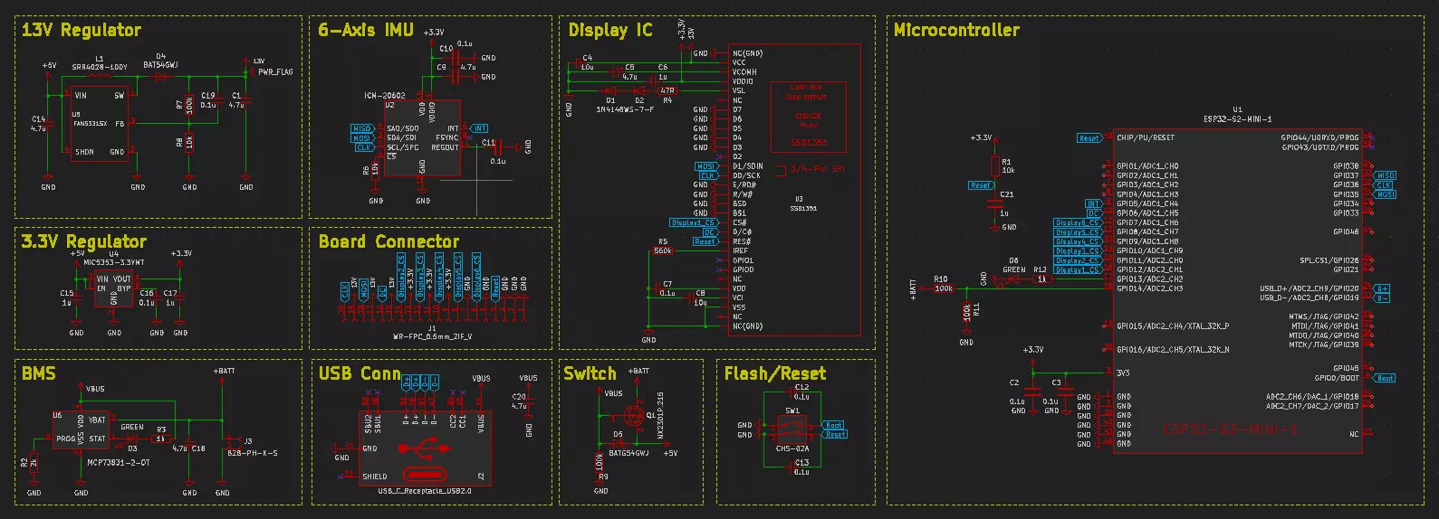
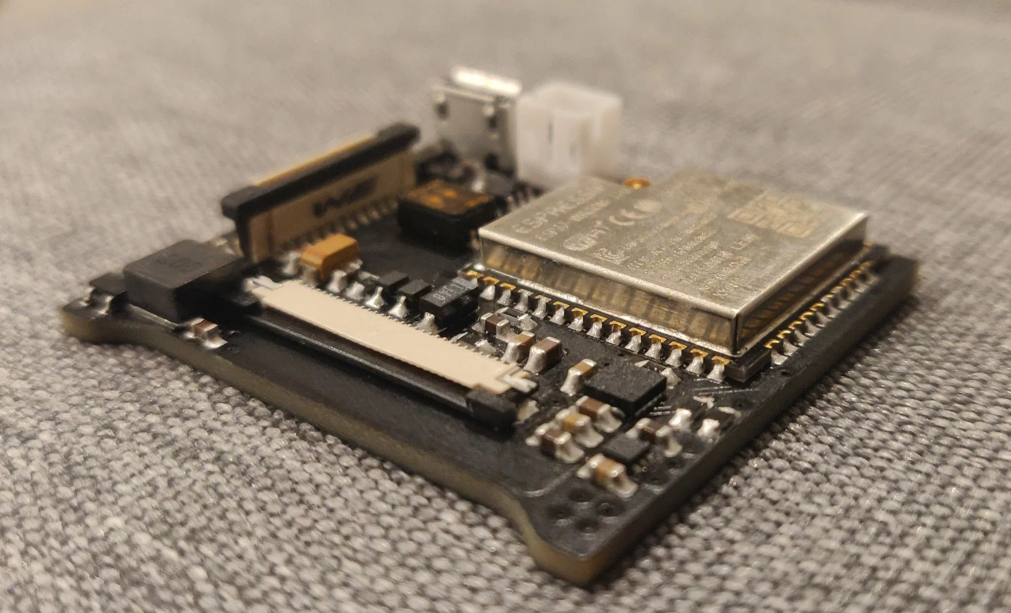
There are 3 main ICs present on the motherboard.
SSD1351
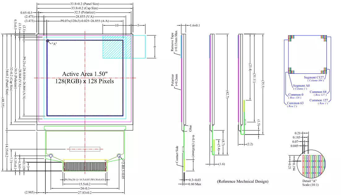
This is the IC used by every display in this design, it allows for SPI control of a 128×128 RGB OLED display. Unfortunately there isn’t a massive market for square OLED displays, so it’s hard to find ones that are small and high resolution. As a result the best display I could find has rather large bezels, hopefully with the growth of the VR market, small OLED screens might become a cheap as phone screens are today.
ICM20602
The ICM20602 is an Inertial Measurement Unit (IMU), housing an accelerometer and gyroscope. IMUs open up the possibility of using simple gestures to control the device, for example shaking the device can be used to wake the device from sleep or tilting the device to control the movement of a cursor. I chose this chip for its small size and SPI port, meaning only one more chip select line needs to be added to the SPI bus used by the displays.
ESP32-S2-Mini-1U
Finally, the star of the show. The ESP32 is an amazing chip for its size, the benefit of using the newer/slightly slower chip is its simplicity. The ESP32-S2 has its own native USB interface, this means I don’t have to add a CP2102 and a bunch of other circuity to my design. Fewer parts, fewer problems.
Daughterboards (PCB 2-6)
The other 5 PCBs have almost identical schematics, providing the passive components and connectors for the displays. These displays will all be daisy-chained together with the motherboard to provide a 6 display device.
Frame Design
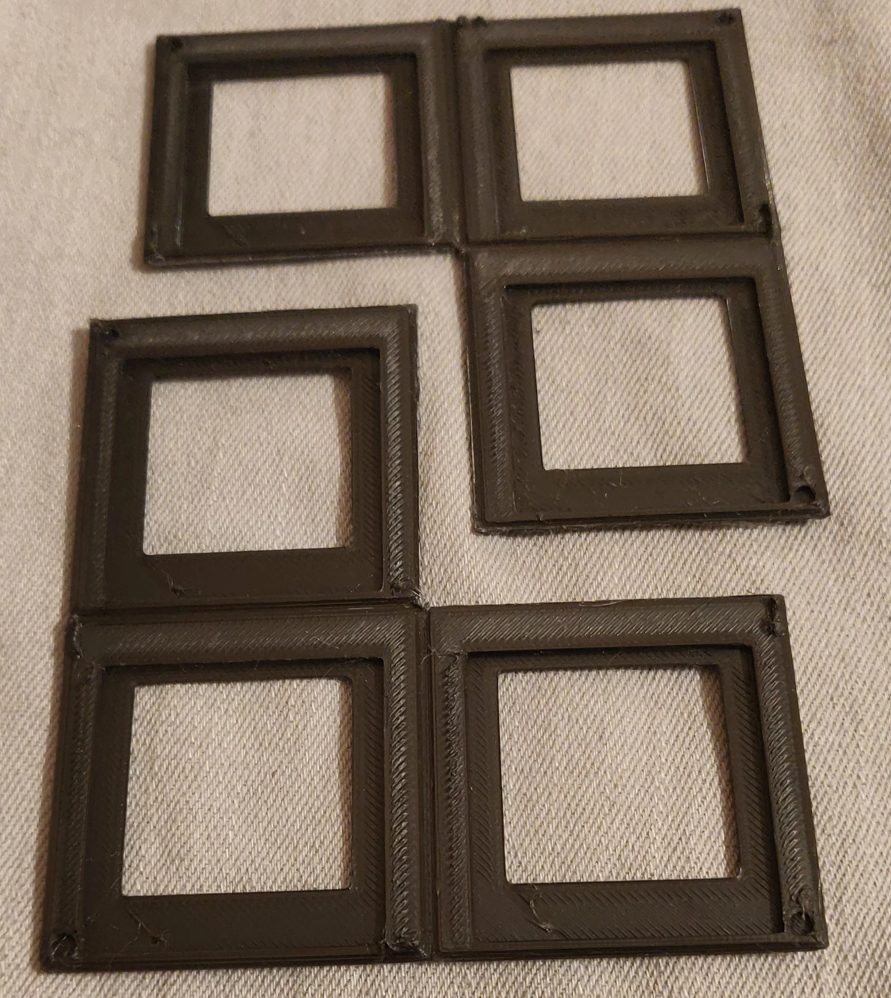
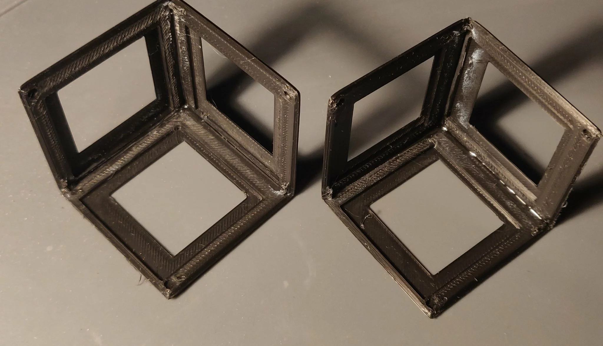
One design idea was to build the frame from two 3 sided pieces which would be joined via 3 mm neodymium magnets. By attaching two halves together the design is easy to charge/fix. I prototyped this frame using ABS on an FDM printer, by printing the pieces flat, I can avoid overhangs and give the outside of the frame a smooth texture. This print can then be folded like origami. The downside of FDM is it’s not very pretty and the tolerances are a bit too high for a print of this scale, so whilst the origami method works well, it makes the frame look amateurish.
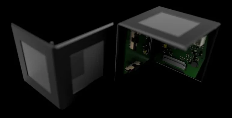
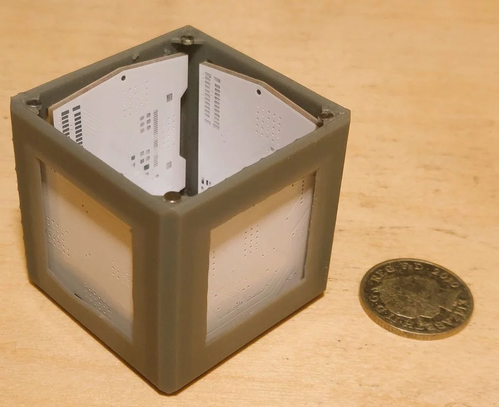
I also tried a lid design, where the design would be printed as a single piece, with one panel being attached with the 3 mm magnets. Whilst I liked the speed and quality of the SLA print, it was very brittle, leading to parts chipping during clean-up of the supports. Another issue with the design is it would be hard to place PCBs with 5 panels connected.
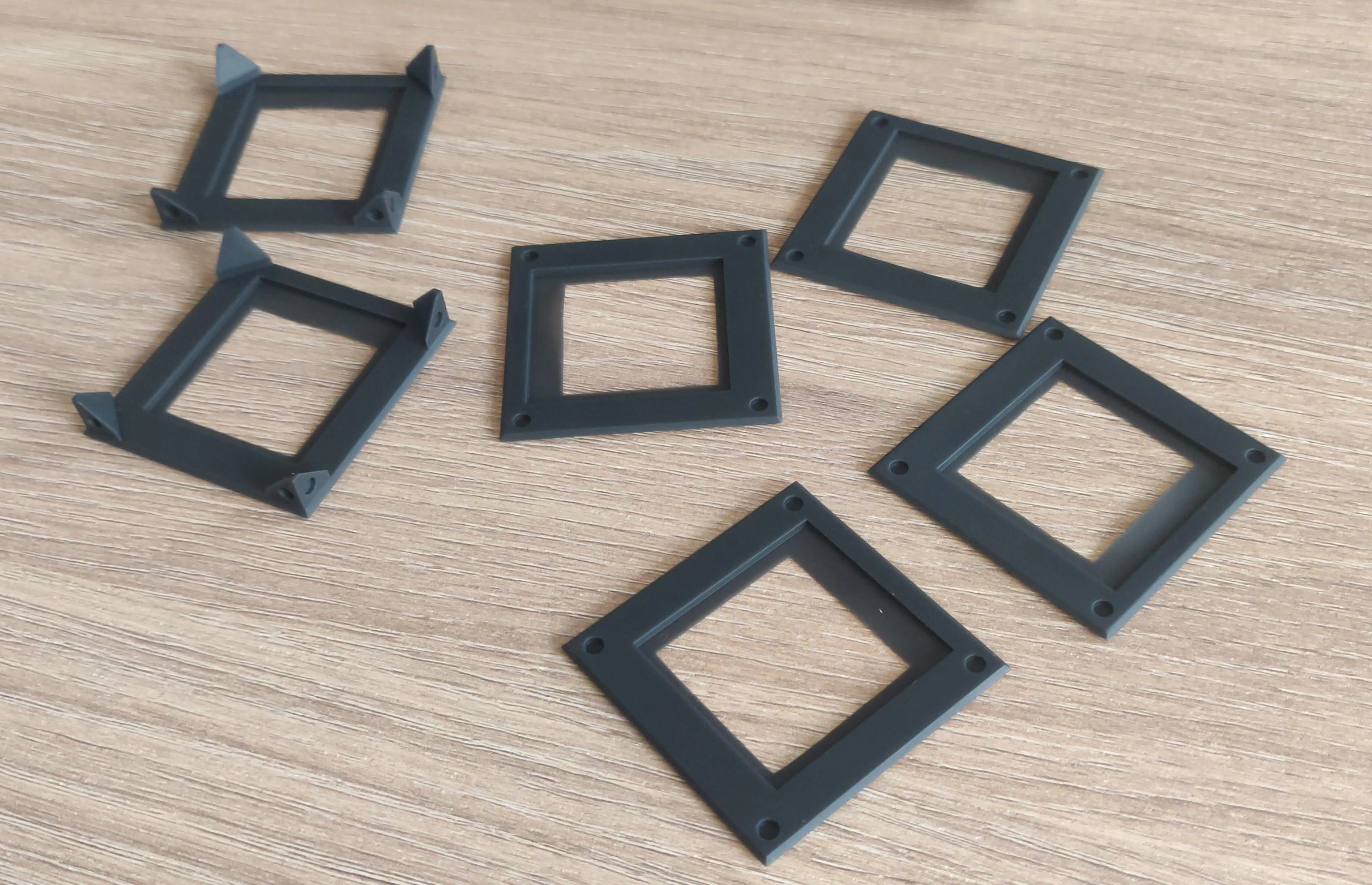
Finally, I experimented with printing the frames as individual panels, allowing for PCBs and screens to be easily attached. The parts were sent to JLCPCBs new 3D printing service, removing a lot of the hassle and ensuring an amazing quality print. This design was the highest quality I have made so far, however using magnets for each frame resulted in a much more fragile design. The magnets hold extremely well until pressure on opposite corners of the cube is applied, resulting in a pealing motion which separates the magnets with ease. The other issue is the amount of magnets that have to be placed and the difficulty of gluing them to the frame.
I came up with multiple designs for the frame, but what I ultimately decided was the frame should be made of at least two evenly sized pieces in order to separate easily for charging/fixing the device. If any frame piece has more than 3 sides, it becomes hard to assemble.
The final design will likely incorporate aspects of all 3 of these prototypes, using 3 sided pieces, printed in SLA from JLCPCB, and using the improvements to the magnet cutouts.